 English
 Pусский
 Français
 Español
 Portugues
 Deutsch
 lingua italiana
 العربية
 Melayu
 Filipino
 Монгол хэл
 dansk
dansk Bahasa indonesia
 日本語
日本語 한국어
한국어 Türk dili
 Tiếng Việt
 svenska
 Nederlands
 Norsk språk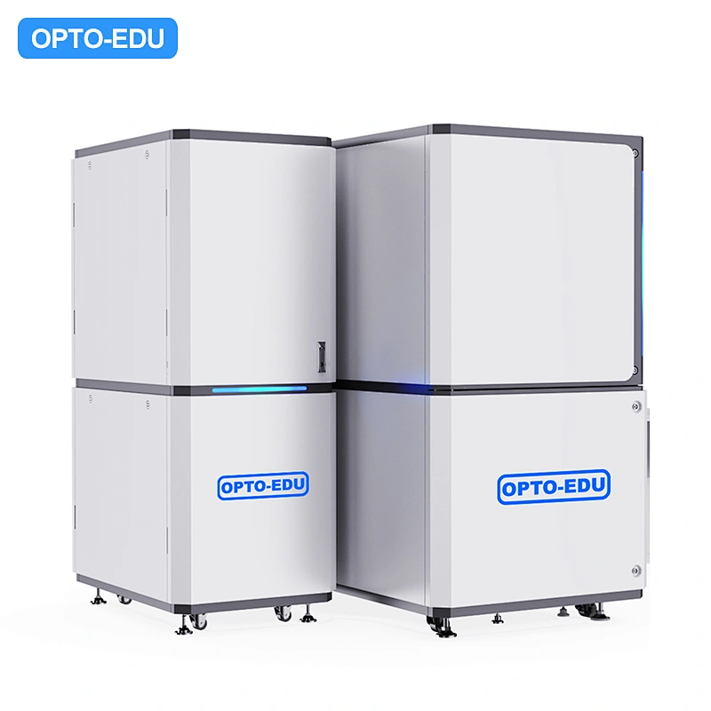

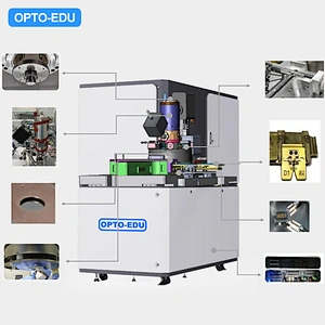

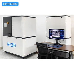

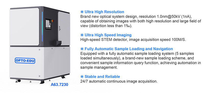
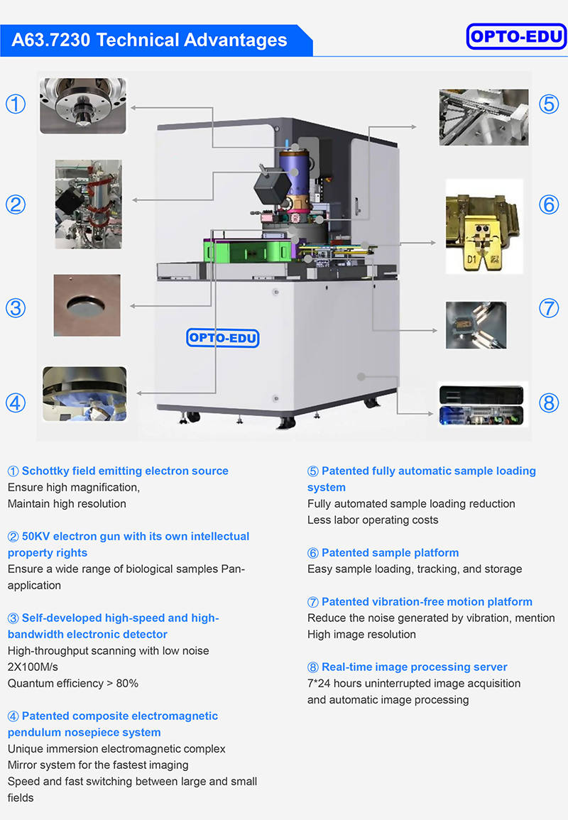
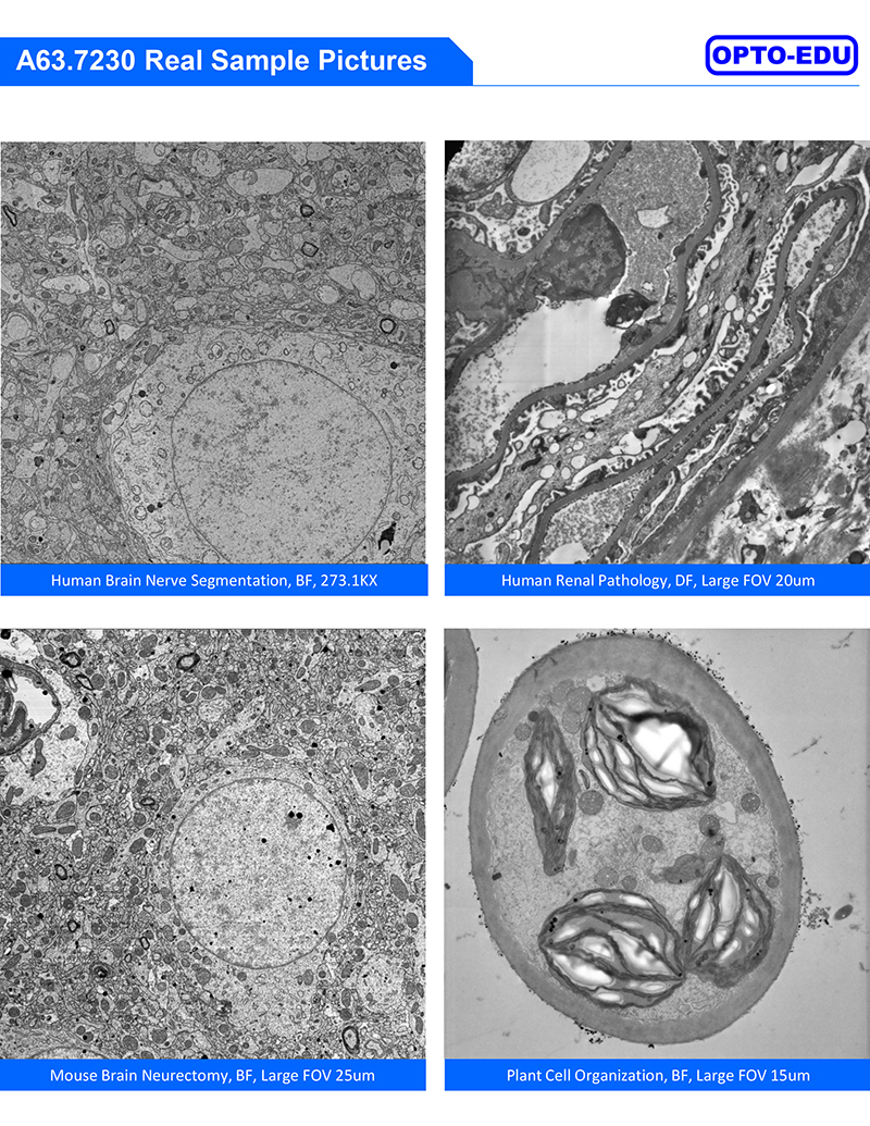
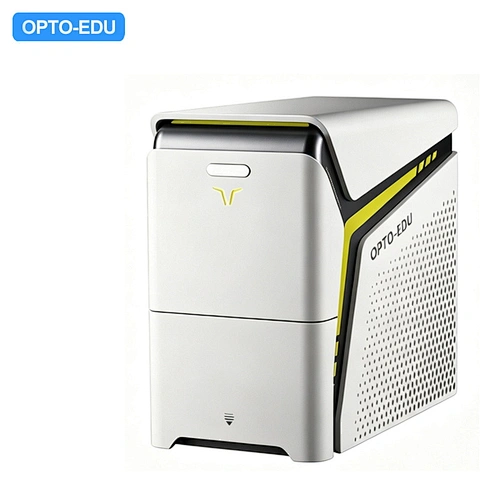
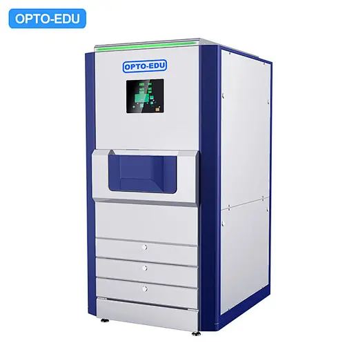
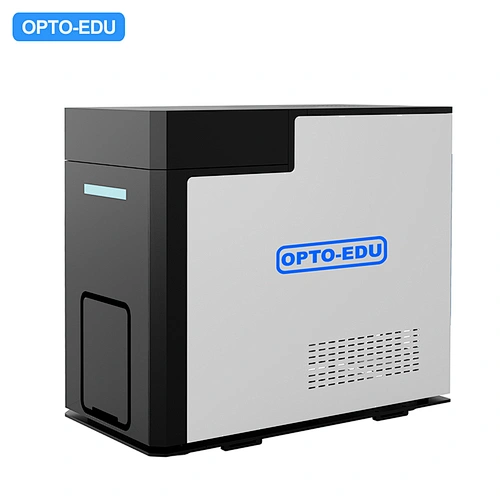
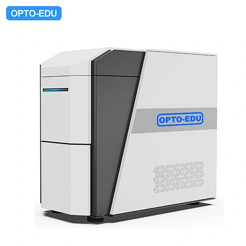
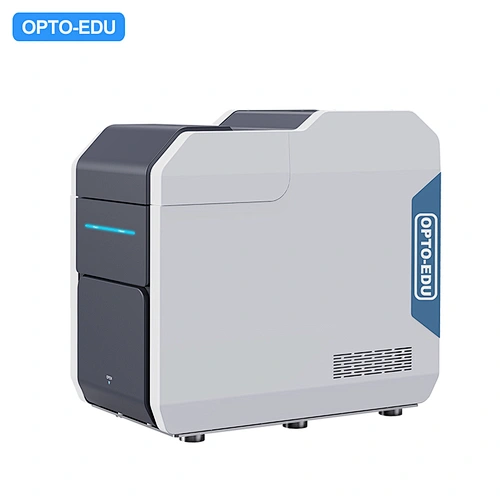
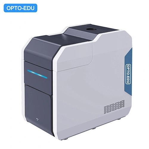
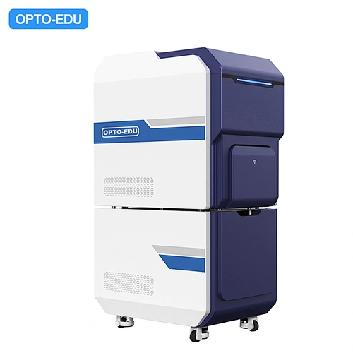
Rapid Automatic Micro-Particle Imaging Analysis System A63.7230 is a fast, intelligent, fully automated scanning transmission electron microscope (STEM) with complete independent intellectual property rights at 50KV. It meets the application needs in fields such as virus morphology observation, vaccine cell bank safety testing, vaccine research and manufacturing, clinical pathological tissue slice research, and biological research on brain neural connect omics. |
A63.7230 Core Technology | |
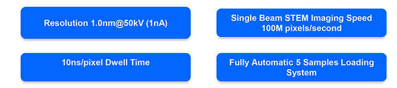
◉ High Resolution High Brightness Electron Optical System 100M/s ultra high-speed imaging at 50KV. The system has video-level (25fps@2k*2k) nanoscale analysis capability, allowing for fully automated information acquisition without omissions while maintaining high resolution. ◉High Sensitivity Direct Electron Detector All detectors of A63.7230 use independently designed direct electron detectors, which convert electrons directly into electrical signals, achieving a detection efficiency of over 80% and a higher signal-to-noise ratio (SNR). ◉Rapid Switching Between Large Field and High-Resolution Imaging Innovative electron optical design allows large field imaging and high-resolution imaging to operate independently, enabling rapid switching, precise particle identification and positioning, and quick high-resolution imaging. ◉High Speed and High Stability Mechanical Motion Platform Uses a vibration-free motion platform, X=±4mm, Y=±4mm, positioning accuracy 1um. | |
| A63.7230 Transmission Scanning Electron Microscope (STEM) | |
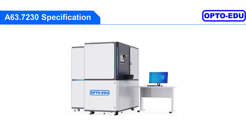
| Resolution | 1.0nm@50kV |
| (1nA beam current, under optimal conditions) | |
| Imaging Mode | BF/DF (Bright Field/Dark Field) |
| STEM Mode Landing Voltage | 50KV |
| Detector Type | Semiconductor Direct Detector |
| Magnification | 1X-500X (Low Magnification Optical Imaging) |
| 500X - 800,000X (STEM Images) | |
| Electron Gun | Schottky Type Thermal Field Emission |
| Electron Beam Current | 50pA to 100nA |
| Sample Stage | X=±4mm, Y=±4mm, Positioning Accuracy 1um |
| Imaging Flux | Can complete imaging of a 1x1mm² area at 4nm pixel within 0.5 hours |
| Ultra High-Speed Image Acquisition | 100MB/s, a single 24k x 24k image takes only 6.5s to capture |
| Acquisition Method | STEM Bright Field (BF) or Dark Field (DF) Acquisition |
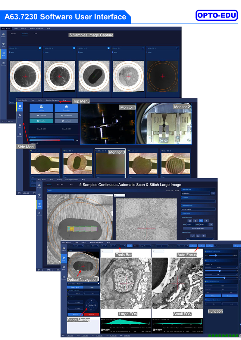
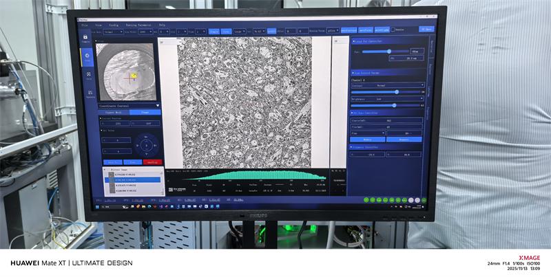
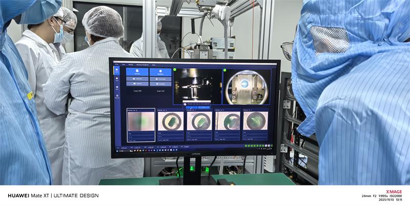
| High Throughput Electron Microscope Control Software | Equipped with automatic image optimization, intelligent focus tracking, panoramic optical navigation, and large area fully automated acquisition functions |
| Rapid Switching Between Large Field and High-Resolution Imaging | Innovative electron optical design, independent operation of large field imaging and high-resolution imaging, rapid switching, precise particle identification and positioning, rapid high-resolution imaging |
| Image Analysis Processing Software AI Server | Ultra-large field imaging, 100um@25nm, AI Server high efficiency recognition and measurement |
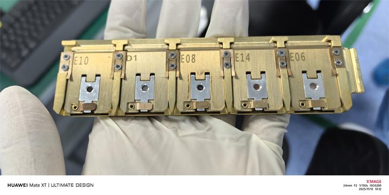
| High Throughput Particle Quantitative Detection Capability | Brand new sample loading system and automated sample management system, ensuring quantitative detection |
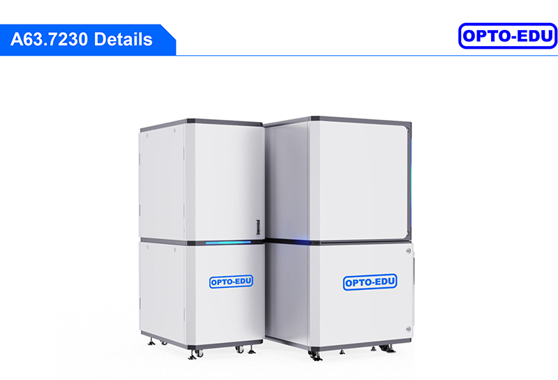
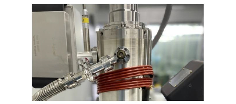
▶Optical System Designed for Fully Automated Micro Particle Detection Traditional transmission electron microscopes have a small field of view, which cannot meet the detection and identification needs of a large number of nanoparticles. A63.7230 is designed based on semiconductor industrial-grade electron beam detection equipment concepts, achieving high-throughput nanoparticle detection capabilities. A63.7230 achieves ultra high-speed imaging through innovative designs such as fast imaging technology, vibration-free sample stage, high-speed electron optical system, and AI technology, with imaging speeds reaching dozens of times that of traditional electron microscopes. |
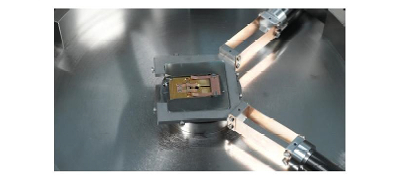
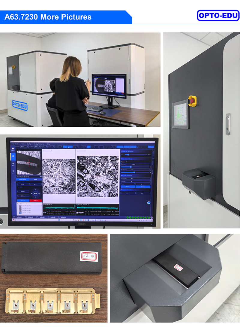
▶Fully Automated Design A series of actions such as power-on inspection, navigation positioning, one-click centering, focus adjustment, and shift correction are automated. The real-time focus tracking system is composed of hardware and software. Using precise electronic deflection to achieve accurate positioning of sample images, resulting in high repeatability of results. It not only eliminates the need for extensive effort to adjust and locate sample positions but also utilizes AI intelligence for automatic detection, ultimately achieving unattended continuous operation. |
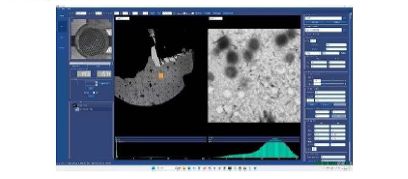
▶Customizable Software Functions for Different Clients Leveraging modern artificial intelligence, AI algorithms, etc., to assist experimental personnel in analysis, from front-end sample preparation to automatic full-section imaging and stitching by the electron microscope, generating high-resolution maps, and then to back-end data processing. AI intelligent analysis can be used for automatic detection and classification of particles, providing users with a complete solution. |




 Huang Xin