 English
 Pусский
 Français
 Español
 Portugues
 Deutsch
 lingua italiana
 العربية
 Melayu
 Filipino
 Монгол хэл
 dansk
dansk Bahasa indonesia
 日本語
日本語 한국어
한국어 Türk dili
 Tiếng Việt
 svenska
 Nederlands
 Norsk språk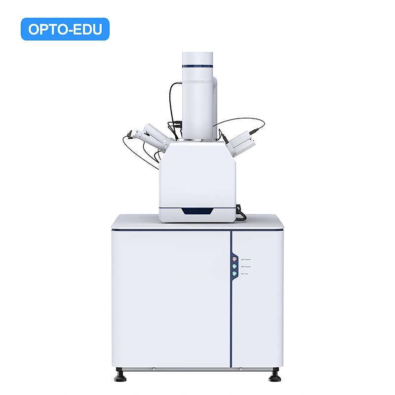




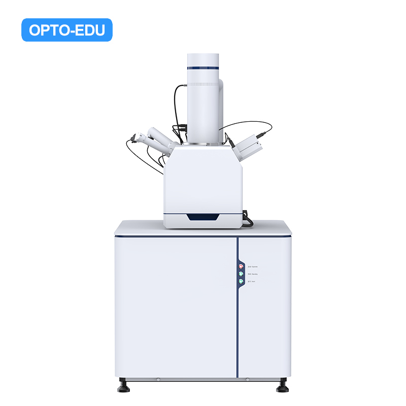

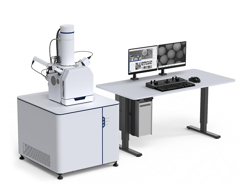
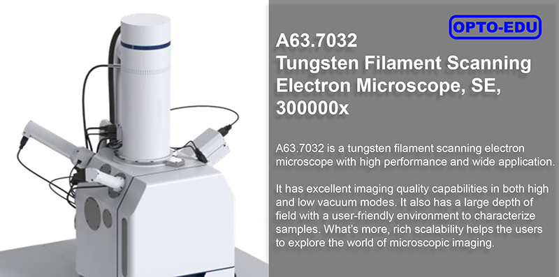
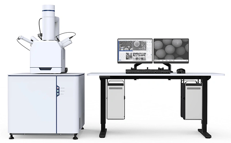
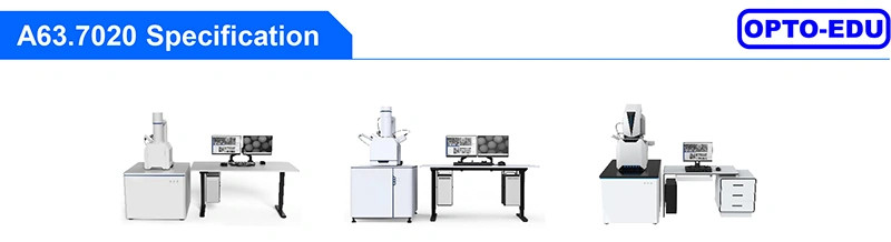
| Specification | A63.7020 | A63.7032 | A63.7050 | |
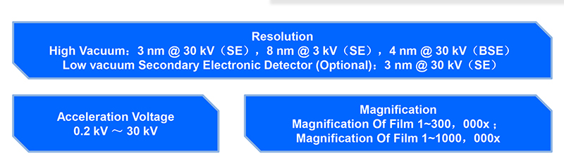
| Resolution | 3.9nm @20kV(SE) 4.5nm @20kV(BSE) | 3nm @30kV(SE) 4nm @30kV(BSE) 8nm @3kV(SE) | 1.0nm @15kV(SE) 1.5nm @1kV(SE) 0.8nm @30kV(STEM) | |
| Voltage | 0.5kV~20kV Optional 30kV | 0.2kV~30kV | 20V~ 30kV | |
| Magnification | 1x~300,000x | 1x~300,000x(film) 1x~1,000,000x(screen) | 1x~ 2,500,000x | |
| Electron Gun | Pre-Aligned Tungsten Filament | Pre-Aligned Tungsten Filament | Schottky Field Emission Electron Gun, With In-cylinder Deceleration, Electromagnetic Composite Objective, Water-cooled Thermostatic Objective | |
| Vacuum System | Fully Auto Control Oil Free Vacuum <5×10⁻⁴ Pa | Fully Auto Control Oil Free Vacuum <5×10⁻⁴ Pa Optional Low Vacuum 5~1000Pa | Fully Auto Control Oil Free Vacuum Electron Gun <9x10⁻⁸Pa Sample Room <5x10⁻⁴Pa | |
| Vacuum Pump | Mechanical pump×1, >200 L/min Turbo molecular pump×1, > 240 L/S | Mechanical pump×1, >200 L/min Turbo molecular pump×1, > 240 L/S | Mechanical pump×1, >6m3/h Turbo molecular pump×1, > 240 L/S, Ion pump x2, >25L/s | |
| Working Stage | 2 Axes Auto Stage, X:100 mm Y:100 mm | 5 Axes Auto Stage, X:120 mm Y:115 mm Z:50 mm T: -10° ~+90° R: 360° Optional3 Axes Auto Stage, A63.7032-A | 5 Axes Auto Stage, X:120 mm Y:115 mm Z:50 mm T: -10° ~+90° R: 360° | |
| Camera | Vertical Optical Navigation CCD | Vertical Optical Navigation CCD Horizontal Monitoring CCD | Vertical Optical Navigation CCD Horizontal Monitoring CCD | |
| Detector | Secondary Electron Detector (ETD) | Secondary Electron Detector (ETD) | Secondary Electron Detector (ETD) High Angle Electron Detector Inlens | |
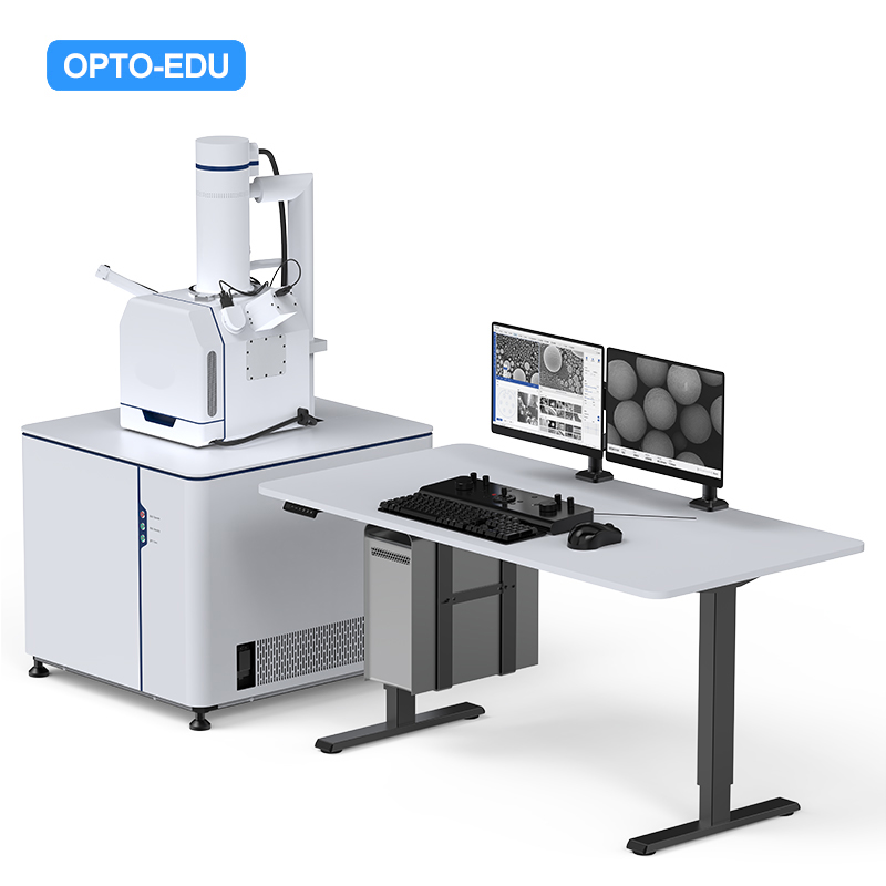
| Software | SEM Operation Software, Language Chinese/English, Mutli Channel Display, Optical Navigation, Gesture Navigation, Auto Brightness Contrast, Auto Focus, Auto Astigmatism, Image Format TIFF,JPG,BMP,PNG | |||
| Computer | Working Station, Memory 16G, Hard Disk 512G, 24"Monitor, Win10 System | |||
| Install Room | L>3000 mm, W>4000mm, H>2300 mm, Temperature 20~25 ℃, Humidity<50% | |||
| Power Supply | AC 220 V(±10 %),50 Hz,2 kVA | |||
| Optional Accessories | Cata. No. | |||
| Optional | BSE | BSE | BSE | A50.7051 |
| EDS | EDS | EDS | A50.7052 | |
| - | EBSD | EBSD | A50.7053 | |
| - | - | EDS+EBSD | A50.7054 | |
| - | - | STEM, 9-quadrant, total area 80mm2 | A50.7055 | |
| - | - | EBIC | A50.7056 | |
| - | - | CL | A50.7057 | |
| - | - | Knob Control Panel & Trackball | A50.7058 | |
| - | - | Sample Exchange Warehouse | A50.7059 | |
| - | - | Beam Gate & Electron Beam Exposure | A50.7060 | |
| - | LVD, Low Vacuum Detector | - | A50.7061 | |
| - | Double Anode (Tetrode Emission) | - | A50.7062 | |
| Tungsten Filament(6pcs) | Tungsten Filament(6pcs) | - | A50.7063 | |
| Large Size Image Stitching Software | Large Size Image Stitching Software | Large Size Image Stitching Software | A50.7070 | |

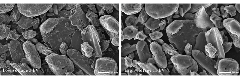
▶Low Voltage For carbon material samples, at low voltage, the penetration depth is small, and the true morphology of the sample surface can be obtained with richer details. |
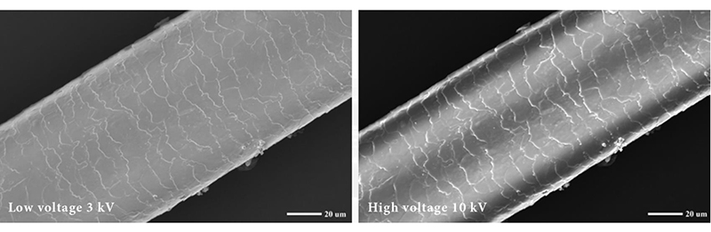
For hair samples, at low voltage, the damage of electron beam irradiation is reduced and the charge effect is eliminated. |
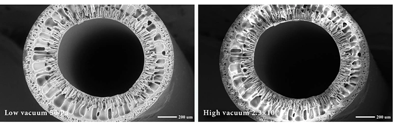
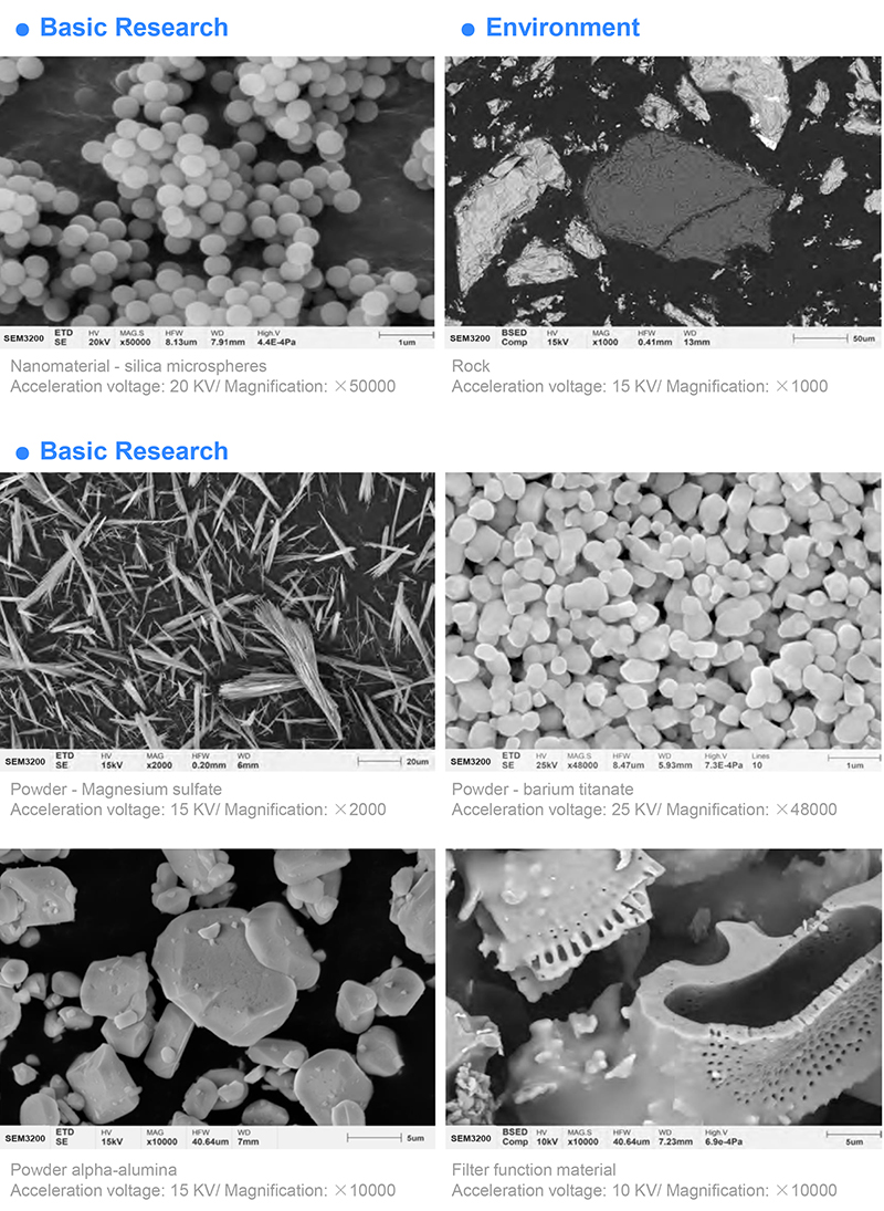
▶Low Vacuum (Optional) The filter fiber tube material has poor electrical conductivity and obvious charge under high vacuum. Under low vacuum, the non-conductive sample can be directly observed without coating. |
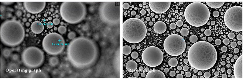
▶Feature Function Intelligent Assisted Astigmatism Directly reflect the astigmatism of the whole field of vision, through the mouse click clear, can quickly adjust the astigmatism to the best. |
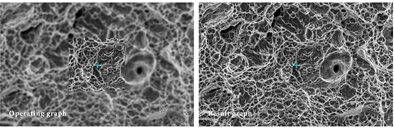
Autofocus One-click focus for fast imaging. |
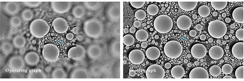
Automatic Astigmatism One-click astigmatism, improve efficiency. |
Automatic Brightness Contrast One-click automatic brightness contrast, gray level appropriate image. |
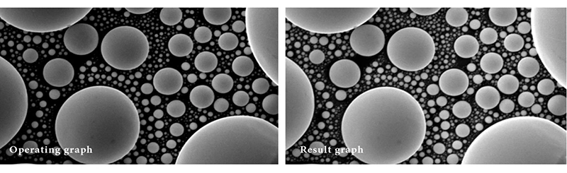
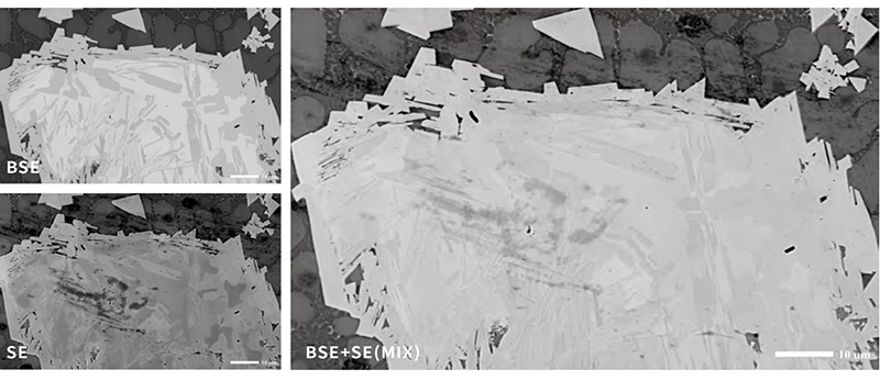
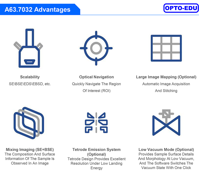
Image Multiple Information Simultaneously A63.7032 supports one-click switching between SE and BSE hybrid imaging, the morphology and composition information of samples can be observed simultaneously. |
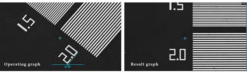
Fast image Rotation Drag a line and the image is instantly"angled“. |
▶Wide Field Of View Biological samples can easily obtain the overall morphology and head structure details of the ladybug by using widefield observation, and display cross-scale analysis. |
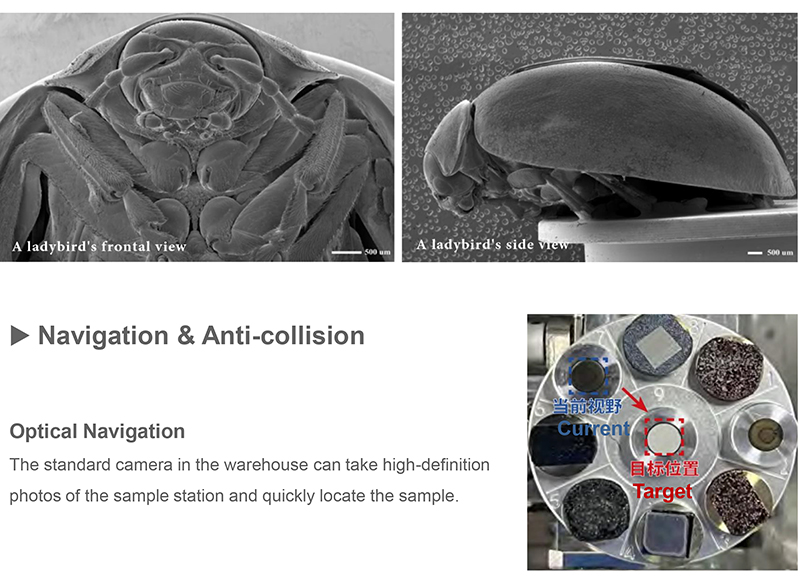
Gesture Shortcut Navigation Box selection and magnification: under the low-power navigation, you can get a large field of view of the sample, which can quickly select the sample area you are interested in, improving work efficiency. |
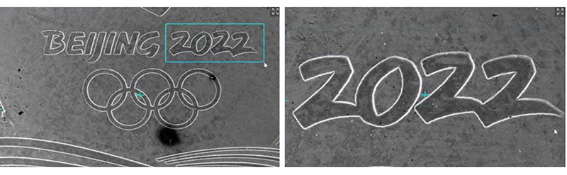

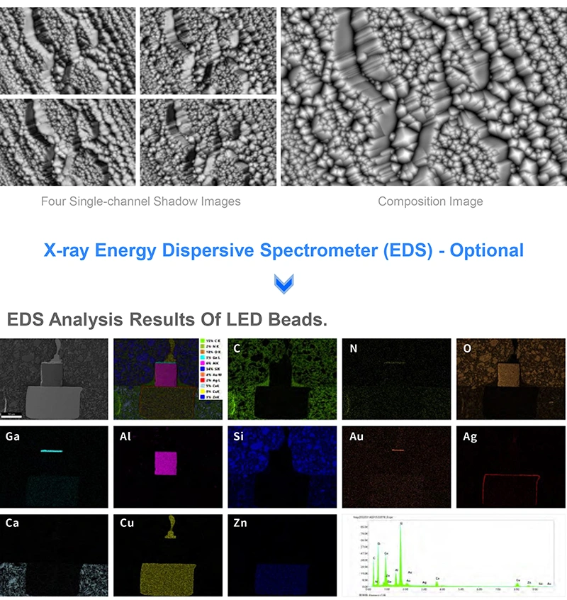
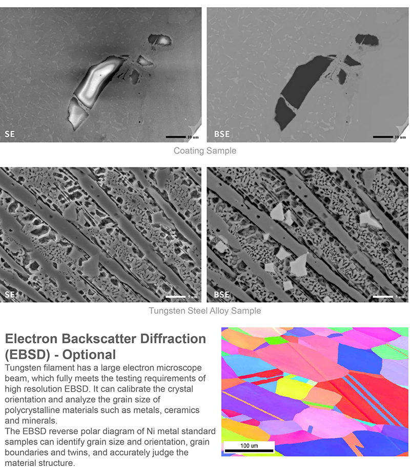
Scanning electron microscope is not only limited to the observation of surface morphology, but also can be used to analyze the micro-components of the sample surface. In addition to conventional secondary electron detector (ETD), backscattered electron detector (BSED), and X-ray energy dispersive spectrometer (EDS), many interfaces are reserved, such as electron backscattered diffraction (EBSD), cathode ray (CL) detectors can be integrated on A63.7032. Quadripartite Backscattered Electron Detector (BSE) -- Multichannel Imaging The detector is exquisitely designed and highly sensitive. It adopts a 4-segment design, and can obtain shadow images and component distribution images in different directions without tilting the sample |

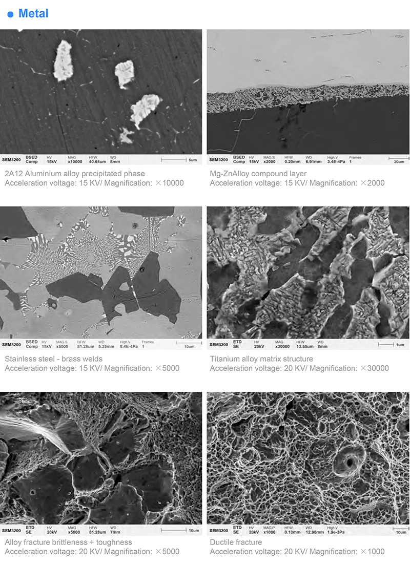
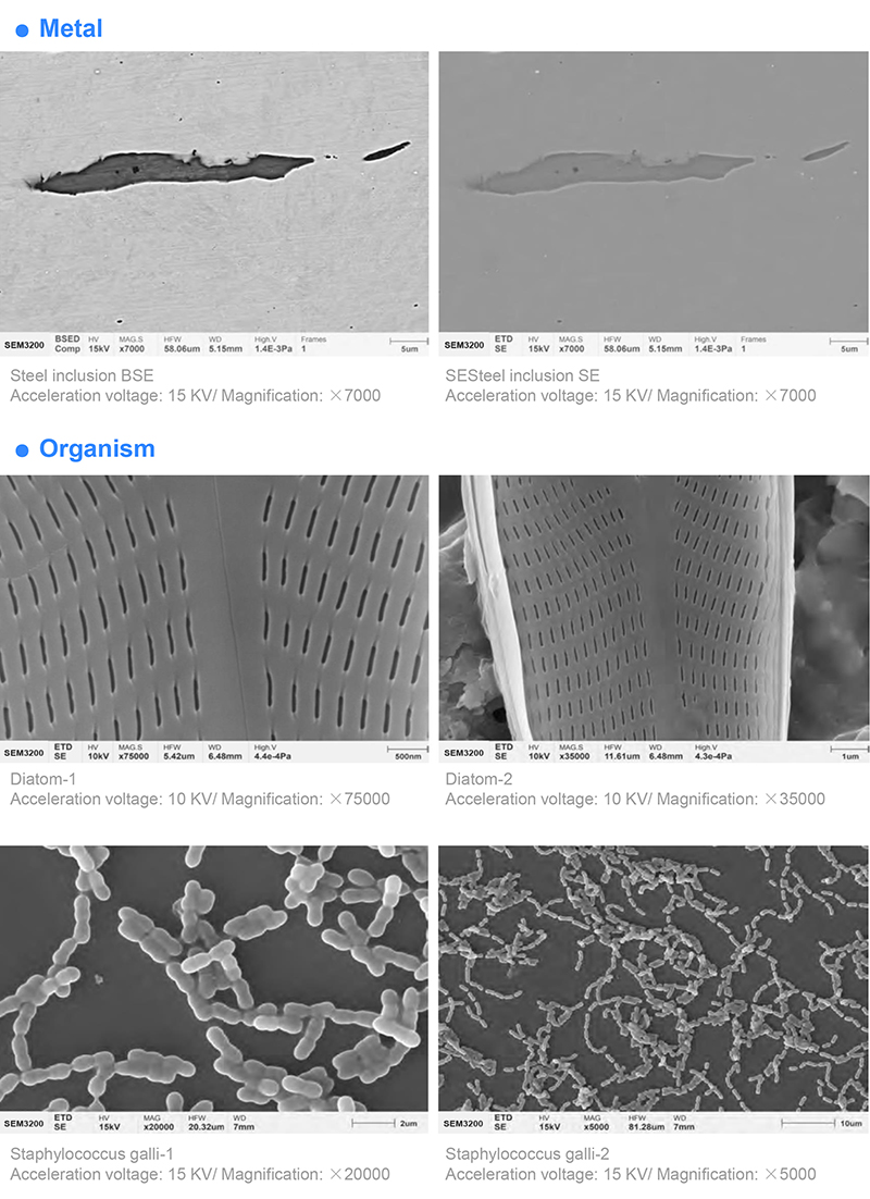
SE image VS BSE image In the backscattered electron imaging mode, the charge effect is weakened obviously, and more composition information can be obtained on the sample surface |
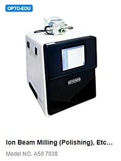
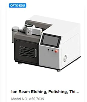
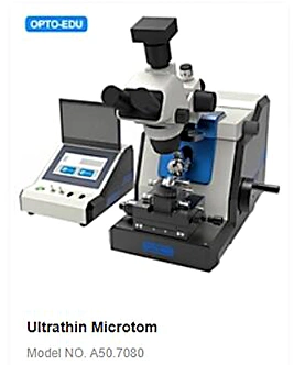
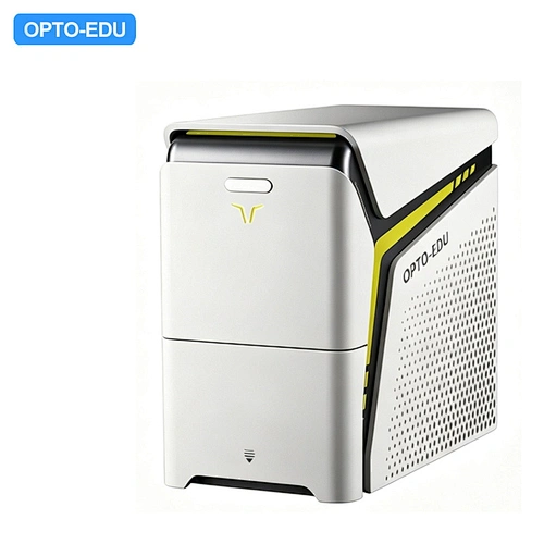
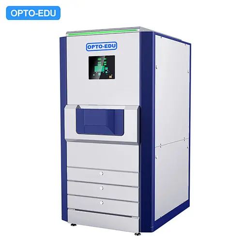
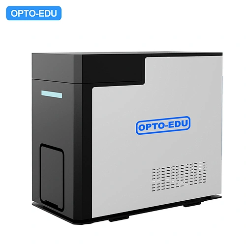
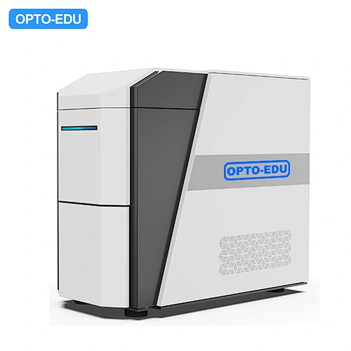
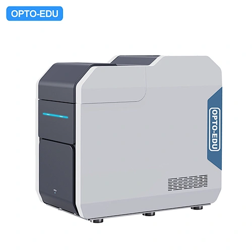
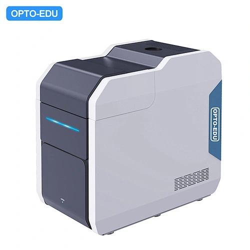
| Scanning Electron Microscope Sample Preparation Instrument | ||
 |  |  |




 Huang Xin