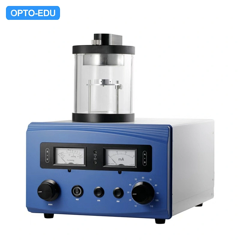
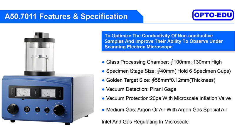
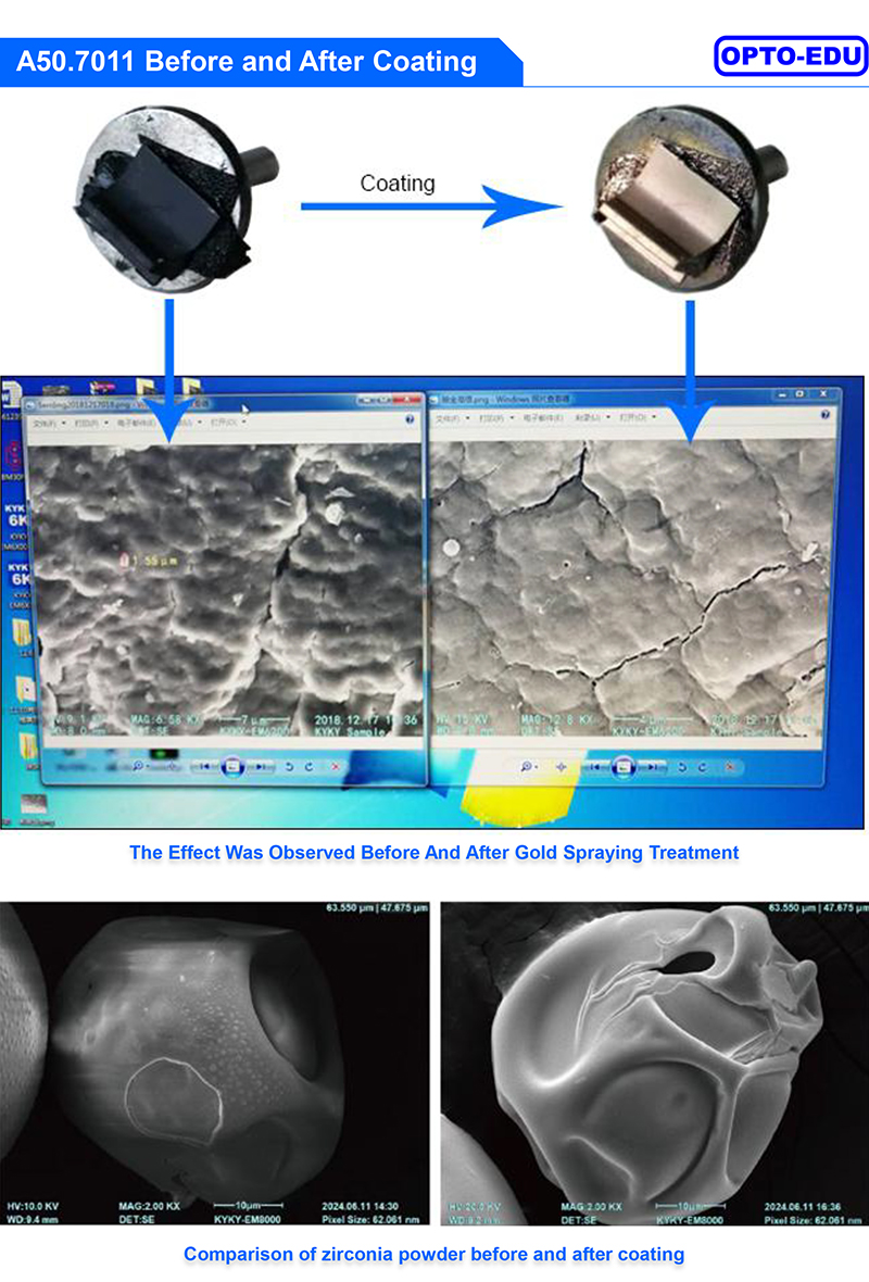
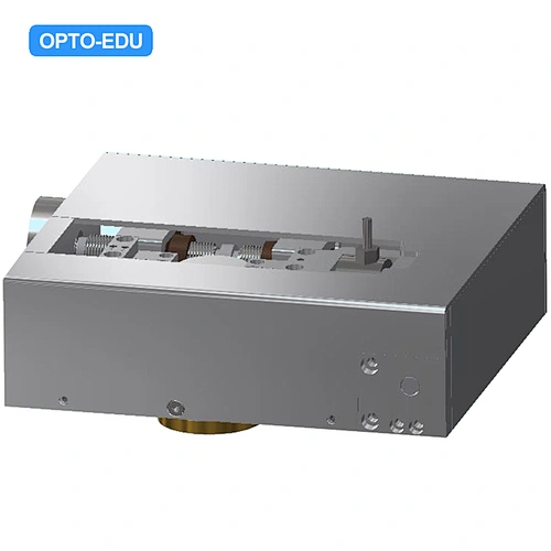
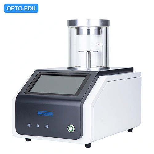
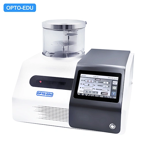
Use 1: SEM sample preparation. A conductive layer of several nanometers to tens of nanometers is plated on the non-conductive sample to improve the surface conductivity of the sample, eliminate charge accumulation, and improve the clarity of electron microscope images.
Use 2: Electrode preparation. A conductive layer of tens of nanometers is plated on the non-conductive substrate to improve the conductivity and serve as the electrode of the battery material.
Applicable samples: no thermal damage to the sample, suitable for all samples
We use cookies on our website to see how you interact with it. By accepting, you agree to our use of such cookies. privacy policy
Advanced Cookie Settings
Essential Cookies
These cookies enable core functionality such as security, verification of identity and network management. These cookies can’t be disabled.
Enable Marketing Cookies
These cookies are used to track advertising performance, consent to the sending of advertising-related user data to Google, and consent for the website to serve personalized advertising to provide more relevant services.
Enable Functional Cookies
These cookies collect data to remember choices users make to improve and give a more personalised experience.
Enable Analytics Cookies
These cookies help us to understand how visitors interact with our website, discover errors and provide a better overall analytics.
 English
 Pусский
 Français
 Español
 Portugues
 Deutsch
 lingua italiana
 العربية
 Melayu
 Filipino
 Монгол хэл
 dansk
 Bahasa indonesia
 日本語
 한국어
 Türk dili
 Tiếng Việt
 svenska
 Nederlands
 Norsk språk







 Huang Xin